

Sitemap Link exchange: Tsinghua Unigroup >
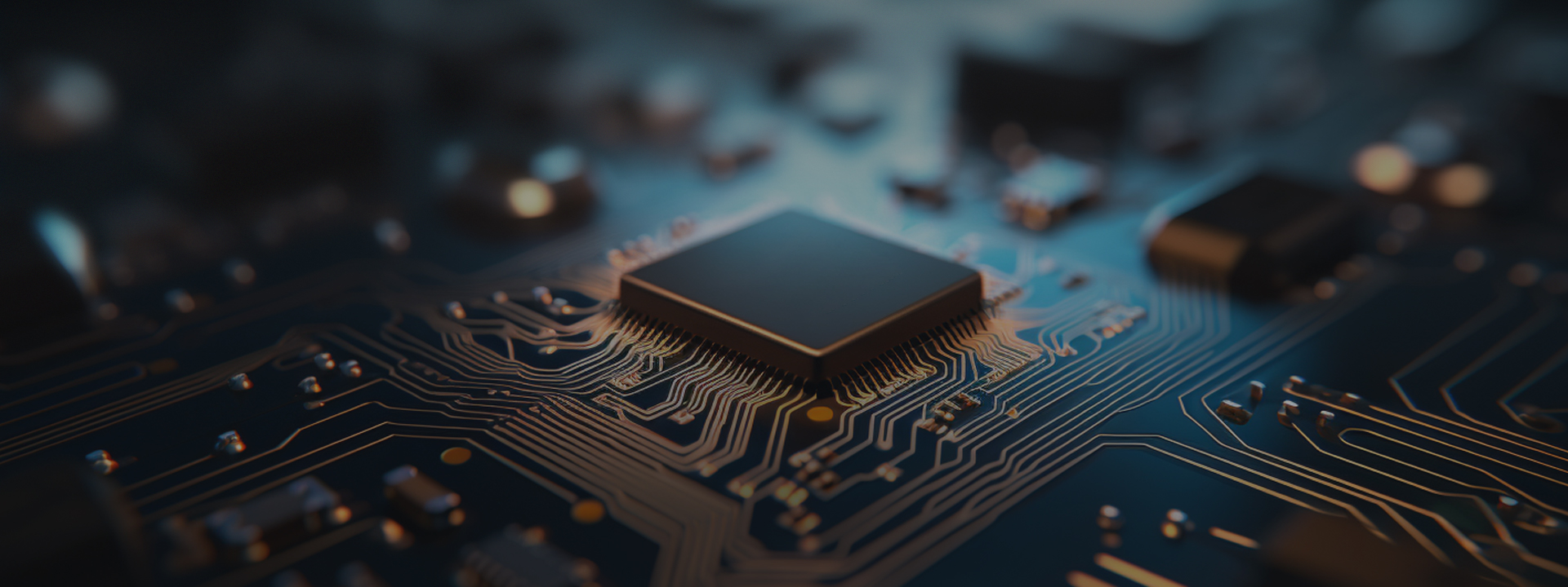
PG2T390H-FFBG900 DEMO Board
2025-09-17
Functional Features:
The board power supply uses a 12V power adapter or a chassis power interface for input.
FPGA: PG2T390H-FFBG900.
CPLD: PGC7KD-MBG400.
Used for FPGA configuration.
Used for controlling FPGA power-on sequence.
Used for configuring the programmable crystal oscillator SI5345.
FPGA Configuration Modes:
Supports JTAG mode.
Supports master SPI mode, using CPLD forwarding to communicate with SPI FLASH.
Supports 16-bit slave parallel configuration mode, with the master device using CPLD.
FPGA Clock Inputs:
1 50MHz single-ended crystal oscillator, connected to the FPGA HR_BANK global clock input pin.
1 100MHz differential crystal oscillator, connected to the FPGA HP_BANK global clock input pin.
The programmable clock source SI5345A can provide REFCLK for the four HSST_HP of the FPGA, and can also provide a global clock for the FPGA HP_BANK.
External SMA interfaces can provide REFCLK for HSST_HP2 and HSST_HP4 of the FPGA.
FPGA Interfaces:
PCIE X8 interface, connected to FPGA_HSST_HP3 and FPGA_HSST_HP4.
Four-channel SFP+, connected to FPGA_HSST_HP2.
DDR4 X64 interface, connected to FPGA HP_BANK.
1 Gigabit Ethernet interface, RJ45 type socket, connected to FPGA HR_BANK.
1 USB to UART interface, MINI B type USB socket, connected to FPGA HR_BANK.
1 FMC expansion interface, connected to FPGA_HSST_HP1, 19 pairs of differential IOs and 8 single-ended IOs of FPGA HR_BANK. It also leads out 12V power supply and 3.3V power supply.
FPGA HR_BANK leads out 10 IOs connected to LEDs, 4 IOs connected to buttons, 8 IOs connected to DIP switches, and 100 IOs connected to pin headers.

- Products Titan Family Logos Family Compa Family Pango Design Suite
- Solutions Communication Industrial Image&Video Consumer Auto Data center Other
- Resource Software and license IP Partners
- About us Company profile Contact us Announcement
-
Contact us
86-755-66886188
marketing@pangomicro.com
No. 15, Gaoxin South Road,
High-Tech Industrial Park,
Nanshan District, Shenzhen
 Official public account

©2023 All Rights Reserved Shenzhen Pango Microsystems Co., Ltd. Guangdong ICP Filing No. 14029535
